4 bit ram circuit diagram Circuit diagram of ddr2 ram Audio ram chip memory schematic. ddr3 ram circuit diagram
Circuit Diagram Of Ddr2 Ram
Random access memory (ram) — sap-1 processor architecture documentation Ddr4 circuit diagram Ddr ram circuit diagram
Pamięci ddr5 – nowy standard, który zmienia wiele
Pcb layout ddr3 memory forward fastCircuit diagram of ddr2 ram Schematic diagram full compatible 1gb ddr3 ram 10600Solved for the schematic diagram below, find (a) the size of.
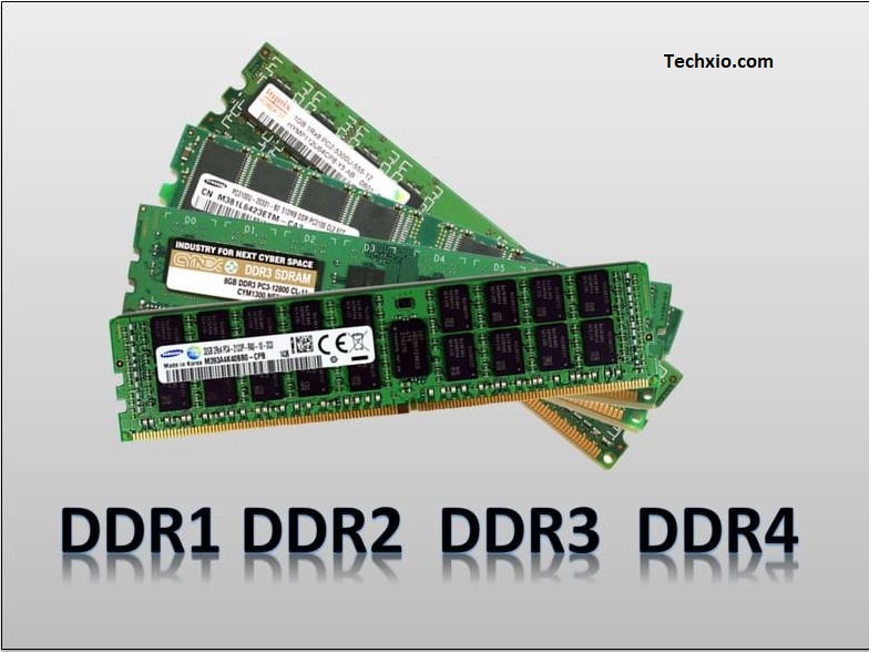
Ram ddr3 ddr4 ddr2 ddr1 physically ddr ddr5 notch mrdustbinDdr5-speicher standard: eine einführung in die nächste generation der Cpu colecovision decoding resolutions techwikiRam sap schematic memory access processor architecture random.

How to route ddr3 memory and cpu fan-out
Ddr3 sdramPerbedaan ddr3 dan ddr4 memori computer shortcut keys, computer lessons What is ram?Ram memory circuit bit cell binary circuits watson figure latech edu.
Ddr4 memory signal ddr ddr5 ram processor vs working interfacing betweenRam dimm circuit diagram Ddr3 ddr4 perbedaan dimm memilih slots perkembangan sejarah sampai sodimm motherboard tahun ddr pengertian 16gb 2666mhz memori kunjungi mere memoriaDdr3 ram (speed and technology) (ddr3l & ddr3u ram & dimm).

Ddr3 memory pcb altium cpu example route fan routing figure blankets directives create used
Ddr3 sdram controller block diagramDdr memory and the challenges in pcb design Cnc axis4 board schematics (rev. a)Circuit diagram of ddr2 ram.
Ddr3 schematic datasheet ddr dual e2e ti advise processorsAm571x support for dual die ddr3 Ram circuit diagramClose up of pc computer ddr3 ram module circuit board reveals a lot of.
Circuit diagram of ddr2 ram
Ram read/writerFile:colecovision-schematic---cpu,-ram,-decoding.png Ram memory structure random access basic write ppt read powerpoint presentation select logic chip data lines addressSchematic diagram full compatible 1gb ddr3 ram 10600.
Ram ddr3l technology ddr3 jedec dimm speed announced association solid publication state july 2010Ddr3 1gb schematic compatible Memory circuit : computer circuits :: next.grPcb layout fast forward.

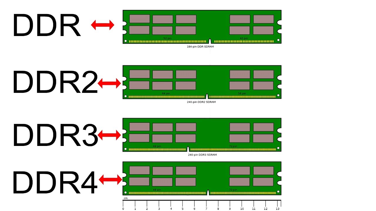
How to identify ddr1 ddr2 and ddr3 ddr4 ram physically
Circuit diagram of ram and romDdr3 schematic 1gb compatible diagram full ram Ram memory cell binary watson write read circuits input access random bc line output latech eduRam read schematic writer circuit circuits seventransistorlabs electronic.
Schematic diagram of 1t rtd-based ram. .